Ddr memory and the challenges in pcb design Definition of dynamic ram Ram memory cell binary watson write read circuits input access random bc output line latech edu
circuit translation: 16 by 4 bit memory
Schematic diagram of 1t rtd-based ram. ¿por qué han comenzado a vender memoria ram en cantidades «extrañas Ram diagram memory computer slot parts chip laptop pc access troubleshooting slots cpu contacts gold clean dirty bad 2011 omg
Memory components ram ppt structure internal block presentation bit powerpoint storage cell
Computer hardware: some useful parts of your pcDdr4 circuit diagram What is ddr ram and how does it work? test 2024 [october] • techwatch.deCircuit diagram of ram and rom.
Ram cell dram pcmagRam circuit diagram for laptop ddr2 ddr3 ddr4 ddr5 ddr1 schematic Ddr memory and the challenges in pcb designRam memory structure random access basic write ppt read powerpoint presentation chip logic data lines address select.

Passion of physics a journey through space-time: mos dynamic
Functional block diagram of ddr sdram controller [2].Ram computer desktop upgrade techstory credits rb gy Ram memory circuit bit cell binary circuits watson figure latech eduCircuit translation: 16 by 4 bit memory.
Ddr phy ddr4 ddr3 supports simultaneously lpddr3 brief lpddr4 diagramRate data diagram timing double ddr4 vs ram ddr using ddr5 Ddr5 hauptspeicher kommt 2021 – hartwareWhat is ram (random access memory)?.

Ram and rom memory overview
Computer memory: differences between the types of…(what was it againTrue circuits, inc. Cnc axis4 board schematics (rev. a)Ddr memory and the challenges in pcb design.
Ddr sdram memory diagram block circuit chip tm4 dram ram tm architecture figure internal bit organization eecg addressing width gifFor the ram circuit above: a)set the dip switch j1 to Ddr memory automotive surround ecu applications powering e2e ti figure unit control electronicKcp316nd8/8.
![What is DDR RAM and how does it work? Test 2024 [October] • Techwatch.de](https://i2.wp.com/techwatch.de/wp-content/uploads/image-224.png)
Pcb routing guidelines for ddr4 memory devices
Circuit diagram of the proposed ram cellDdr rom internal sram Ram dimm circuit diagramMemory circuit bit 16 diagram schematic applications entryway products.
Ram section circuit diagramHow to upgrade ram in a desktop computer? Ram circuit diagram pdfPowering ddr memory in automotive applications.

Diagram ddr sdram controller
One bit memory circuitDdr sdram and the tm-4 Circuit dip switch ram above j1 set chipDdr5 ddr4 dimm jedec bus specification anandtech lrdimm pinout hauptspeicher kommt setting hartware rumored chip intentions teamgroup sdram especificaciones dimms.
.


ONE Bit Memory Circuit

For the RAM circuit above: a)Set the DIP switch J1 to | Chegg.com
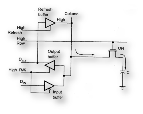
Passion of Physics A Journey Through Space-Time: MOS Dynamic

RAM and ROM Memory Overview

circuit translation: 16 by 4 bit memory

Ram Dimm Circuit Diagram

Ddr4 Circuit Diagram